LTC1704/LTC1704B
7
1704bfa
PI FU CTIO S
U
U
TG (Pin 1): Switcher Controller Top Gate Drive. The TG pin
drives the gate of the top N-channel MOSFET, QT. The TG
driver draws power from the BOOST pin and returns it to
the SW pin, providing true floating drive to QT. TG is de-
signed to typically drive up to 10,000pF of gate capacitance.
SW (Pin 2): Switcher Controller Switching Node. Connect
SW to the switching node of the main converter. The TG
driver ground returns to SW, providing floating gate drive
to the top N-channel MOSFET, QT. The voltage at SW is
compared to I
MAX
by the current limit comparator while
the bottom MOSFET, QB is on. The Burst comparator
(BURST, see Block Diagram) monitors the potential at SW
and switches to Burst Mode operation under light load
conditions.
I
MAX
(Pin 3): Switcher Controller Current Limit Set. The
I
MAX
pin sets the current limit comparator threshold for
the switcher controller. If the voltage drop across the
bottom MOSFET, QB, exceeds the magnitude of the volt-
age at I
MAX
, the switcher controller enters current limit.
The I
MAX
pin has an internal 10礎 current source pull-up,
allowing the current threshold to be set with a single
external resistor to PGND. Kelvin connect this current
setting resistor to the source of QB. Refer to the Current
Limit Programming section for more information on choos-
ing R
IMAX
.
RUN/SS (Pin 4): Switcher Controller Soft-Start. A capaci-
tor from RUN/SS to GND controls the turn-on time and
rate of rise of the switcher output voltage at power up. An
internal 3礎 current source pull-up at RUN/SS sets the
turn-on time at approximately 300ms/礔. If both RUN/SS
and REGILM are pulled low, the LTC1704 enters shutdown
mode.
COMP (Pin 5): Switcher Controller Loop Compensation.
The COMP pin is connected directly to the output of the
switcher controllers error amplifier and the input to the
PWM comparator. Use an RC network between the COMP
pin and the FB pin to compensate the feedback loop for
optimum transient response.
FB (Pin 6): Switcher Controller Feedback Input. FB should
be connected through a resistor divider network to V
OUTSW
to set the switcher output voltage. Also, connect the
switcher loop compensation network to FB.
REGDR (Pin 7): Linear Regulator Controller Driver Output.
Connect REGDR to the base of the external NPN Pass
transistor. The REGILM pin input current controls the
linear regulator controller maximum driving capability.
GND (Pin 8): Signal Ground. All internal low power cir-
cuitry returns to the GND pin. Connect to a low impedance
ground, separated from the PGND node. All feedback,
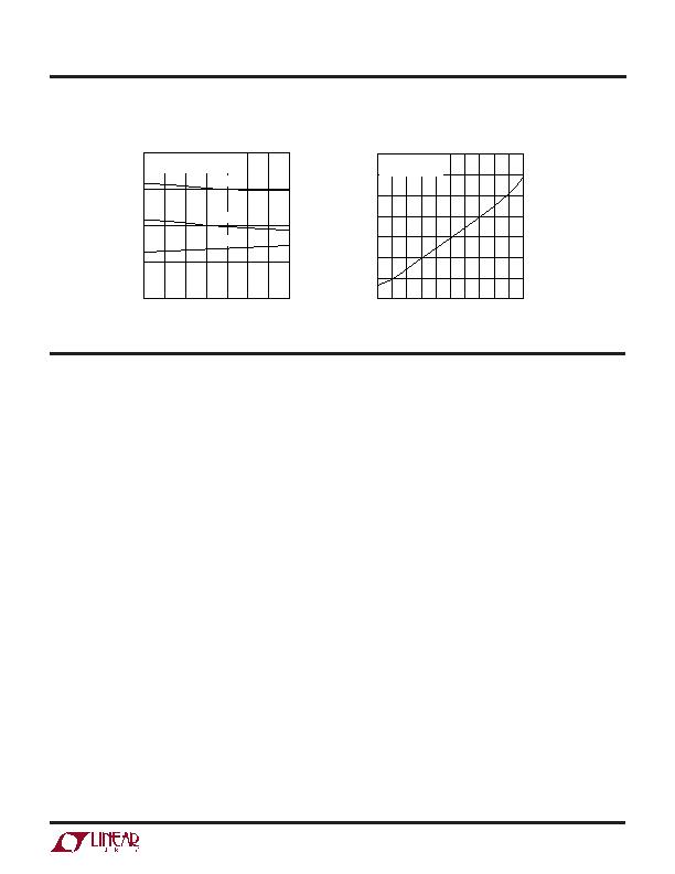
TYPICAL PERFOR A CE CHARACTERISTICS
W
Supply Current vs Temperature
I
PVCC
, I
BOOST
vs Driver Load
TEMPERATURE (癈)
50
0
1.5
3.0
4.5
6.0
25 0 25 50
1704 G26
75 100 125
I
VCC
I
PVCC
I
BOOST
V
CC
= PV
CC
= BOOST = 5V
TG, BG FLOAT
TG, BG LOAD (pF)
0
0
5
15
20
25
35
1704 G27
10
30
4000
10000
2000
6000 8000
T
A
= 25癈
PV
CC
= BOOST = 5V
发布紧急采购,3分钟左右您将得到回复。
相关PDF资料
LTC1966MPMS8#TRPBF
IC RMS/DC CONV MICROPWR 8-MSOP
LTC1967IMS8#TRPBF
IC CONVERTER RMS-DC PREC 8MSOP
LTC1968IMS8#TRPBF
IC CONVERTER RMS-DC PREC 8MSOP
LTC3100EUD#TRPBF
IC REG BUCK/BOOST/LINEAR 16-QFN
LTC3104IMSE#TRPBF
IC REG DL BCK/LINEAR SYNC 16MSOP
LTC3445EUF#TRPBF
IC REG TRPL BUCK/LINEAR 24-QFN
LTC3446IDE#PBF
IC REG TRPL BCK/LINEAR 14-DFN
LTC3537EUD#TRPBF
IC REG DL BST/LINEAR SYNC 16-QFN
相关代理商/技术参数
LTC1705EGN
功能描述:IC PWR SUPPLY CONTROLLER 28SSOP RoHS:否 类别:集成电路 (IC) >> PMIC - 电源控制器,监视器 系列:- 产品培训模块:Lead (SnPb) Finish for COTS
Obsolescence Mitigation Program 标准包装:2,500 系列:- 应用:多相控制器 输入电压:- 电源电压:9 V ~ 14 V 电流 - 电源:- 工作温度:-40°C ~ 85°C 安装类型:表面贴装 封装/外壳:40-WFQFN 裸露焊盘 供应商设备封装:40-TQFN-EP(5x5) 包装:带卷 (TR)
LTC1705EGN#PBF
功能描述:IC PWR SUPPLY CONTROLLER 28SSOP RoHS:是 类别:集成电路 (IC) >> PMIC - 电源控制器,监视器 系列:- 产品培训模块:Lead (SnPb) Finish for COTS
Obsolescence Mitigation Program 标准包装:2,500 系列:- 应用:多相控制器 输入电压:- 电源电压:9 V ~ 14 V 电流 - 电源:- 工作温度:-40°C ~ 85°C 安装类型:表面贴装 封装/外壳:40-WFQFN 裸露焊盘 供应商设备封装:40-TQFN-EP(5x5) 包装:带卷 (TR)
LTC1705EGN#TR
功能描述:IC PWR SUPPLY CONTROLLER 28SSOP RoHS:否 类别:集成电路 (IC) >> PMIC - 电源控制器,监视器 系列:- 产品培训模块:Lead (SnPb) Finish for COTS
Obsolescence Mitigation Program 标准包装:2,500 系列:- 应用:多相控制器 输入电压:- 电源电压:9 V ~ 14 V 电流 - 电源:- 工作温度:-40°C ~ 85°C 安装类型:表面贴装 封装/外壳:40-WFQFN 裸露焊盘 供应商设备封装:40-TQFN-EP(5x5) 包装:带卷 (TR)
LTC1705EGN#TRPBF
功能描述:IC PWR SUPPLY CONTROLLER 28SSOP RoHS:是 类别:集成电路 (IC) >> PMIC - 电源控制器,监视器 系列:- 产品培训模块:Lead (SnPb) Finish for COTS
Obsolescence Mitigation Program 标准包装:2,500 系列:- 应用:多相控制器 输入电压:- 电源电压:9 V ~ 14 V 电流 - 电源:- 工作温度:-40°C ~ 85°C 安装类型:表面贴装 封装/外壳:40-WFQFN 裸露焊盘 供应商设备封装:40-TQFN-EP(5x5) 包装:带卷 (TR)
LTC1706CS8-19
功能描述:IC VID VOLTAGE PROGRAMMER 8SOIC RoHS:否 类别:集成电路 (IC) >> PMIC - 电源控制器,监视器 系列:- 产品培训模块:Lead (SnPb) Finish for COTS
Obsolescence Mitigation Program 标准包装:2,500 系列:- 应用:多相控制器 输入电压:- 电源电压:9 V ~ 14 V 电流 - 电源:- 工作温度:-40°C ~ 85°C 安装类型:表面贴装 封装/外壳:40-WFQFN 裸露焊盘 供应商设备封装:40-TQFN-EP(5x5) 包装:带卷 (TR)
LTC1706CS8-19#PBF
功能描述:IC VID VOLTAGE PROGRAMMER 8SOIC RoHS:是 类别:集成电路 (IC) >> PMIC - 电源控制器,监视器 系列:- 产品培训模块:Lead (SnPb) Finish for COTS
Obsolescence Mitigation Program 标准包装:2,500 系列:- 应用:多相控制器 输入电压:- 电源电压:9 V ~ 14 V 电流 - 电源:- 工作温度:-40°C ~ 85°C 安装类型:表面贴装 封装/外壳:40-WFQFN 裸露焊盘 供应商设备封装:40-TQFN-EP(5x5) 包装:带卷 (TR)
LTC1706CS8-19#TR
功能描述:IC VID VOLTAGE PROGRAMMER 8SOIC RoHS:否 类别:集成电路 (IC) >> PMIC - 电源控制器,监视器 系列:- 产品培训模块:Lead (SnPb) Finish for COTS
Obsolescence Mitigation Program 标准包装:2,500 系列:- 应用:多相控制器 输入电压:- 电源电压:9 V ~ 14 V 电流 - 电源:- 工作温度:-40°C ~ 85°C 安装类型:表面贴装 封装/外壳:40-WFQFN 裸露焊盘 供应商设备封装:40-TQFN-EP(5x5) 包装:带卷 (TR)
LTC1706CS8-19#TRPBF
功能描述:IC VID VOLTAGE PROGRAMMER 8SOIC RoHS:是 类别:集成电路 (IC) >> PMIC - 电源控制器,监视器 系列:- 产品培训模块:Lead (SnPb) Finish for COTS
Obsolescence Mitigation Program 标准包装:2,500 系列:- 应用:多相控制器 输入电压:- 电源电压:9 V ~ 14 V 电流 - 电源:- 工作温度:-40°C ~ 85°C 安装类型:表面贴装 封装/外壳:40-WFQFN 裸露焊盘 供应商设备封装:40-TQFN-EP(5x5) 包装:带卷 (TR)